Training for Laser Decapsulation Systems
As the former lead application scientist for laser semiconductor decapsulation at Control Laser Corporation (CLC) using their FALIT laser IC decapper, I am able to bring my extensive knowledge of this process to assist your team in getting the most out of your semiconductor decapsulation system. During such training, your team will learn:
- How to identify a good laser process compared to a bad laser process, including tell-tale signs of such
- How to develop recipes for the various semiconductor mold compounds
- An understanding on how the laser reacts with various semiconductor materials
- Special techniques to use for challenging materials like ceramics
- Recommended work flow and recipe documentation
- The theory behind laser decapsulation and how to get the most out of your laser decapsulation system, in general
Consulting for Laser Decapsulation Systems
I can provide purchase consulting for the various laser decapsulation systems on the market. With this consulting, you can be assured that you will get the best system configuration for your needs. I can also join you for the acceptance to make sure that the system is up to par before you take delivery.
Laser Decapsulation Experience
From January 2006 until my departure from CLC in December 2017, I worked with many Failure Analysis (FA) customers around the world in helping to dial-in the laser decapsulation process and also to improve the FALIT system with customer feedback. I was the key person at CLC in developing working partnerships with the top labs in understanding the challenges of the FA labs and helping to solve big problems with semiconductor decapsulation.
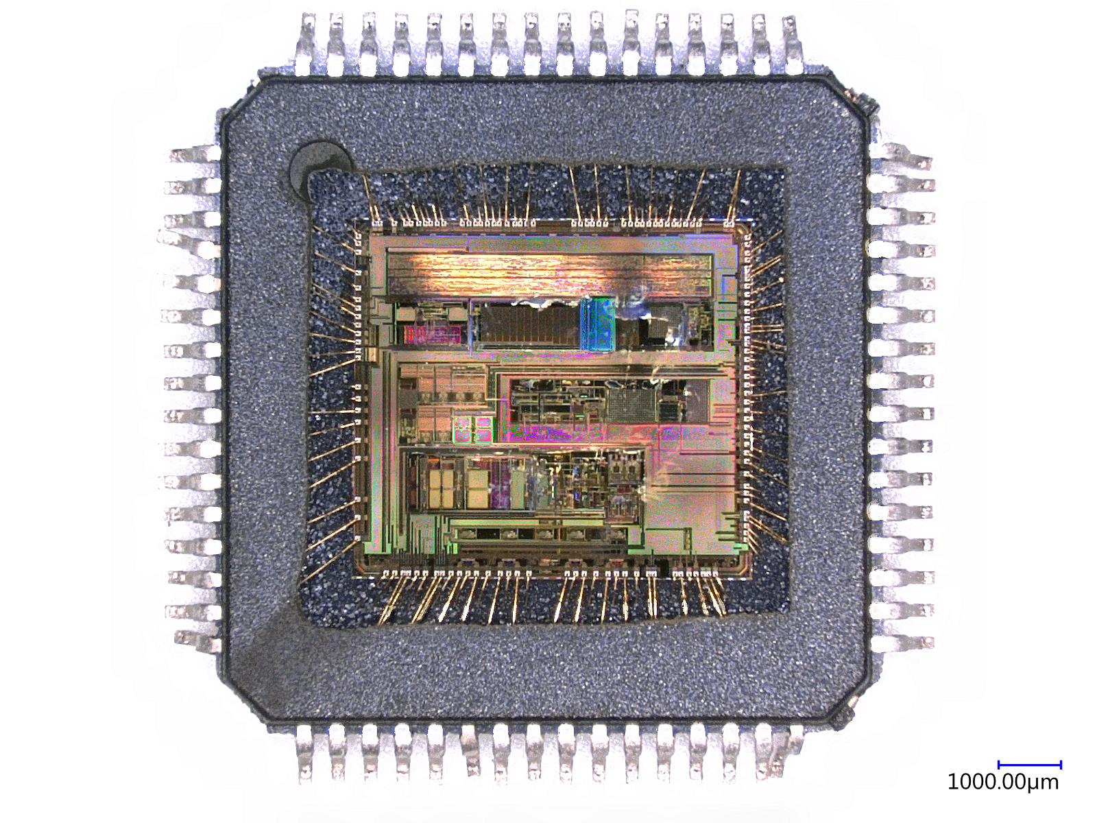
Here is an example semiconductor that has been fully processed–both laser and chemical/acid decapsulation. Courtesy of Analog Devices
At ISTFA 2016, I co-authored and presented a paper titled “Effective Laser Decapsulation Employing the Digital ICO Laser and HAZ-Methodology” with one of our company partners Infineon and Greg B. Anderson. This paper, written in a tutorial format, provides a good foundation on understanding the various parameters in an effort to get as close to the semiconductor die as possible. The results of the paper show an Infineon SOT23 diode that has been laser decapped to the polyimide layer using only laser technology and with test results showing that the laser did not damage the die.
My guidance and valuable insight into this process will expand on this paper to give you and your team a full understanding of the laser decapsulation process. Contact me today and let’s discuss your laser decapsulation consulting and training needs.